1. Graphene Research Institute,Sejong University,Seoul 143-747,Republic of Korea;Faculty of Nanotechnology & Advanced Materials Engineering and Graphene Research Institute,Sejong University,Seoul 143-747,Republic of Korea;2. Graphene Research Institute,Sejong University,Seoul 143-747,Republic of Korea;Department of Physics and Graphene Research Institute,Sejong University,Seoul 143-747,Republic of Korea
Abstract:
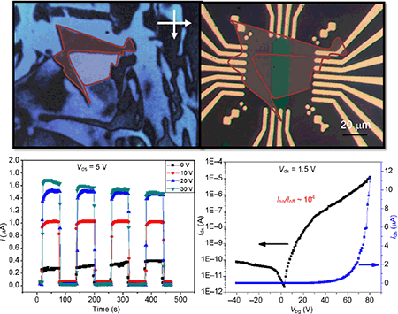
Typically, molybdenum disulfide (MoS2) synthesized by chemical vapor deposition (CVD) is polycrystalline; as a result, the scattering of charge carriers at grain boundaries can lead to performances lower than those observed in exfoliated single-crystal MoS2. Until now, the electrical properties of grain boundaries have been indirectly studied without accurate knowledge of their location. Here, we present a technique to measure the electrical behavior of individual grain boundaries in CVD-grown MoS2, imaged with the help of aligned liquid crystals. Unexpectedly, the electrical conductance decreased by three orders of magnitude for the grain boundaries with the lowest on/off ratio. Our study provides a useful technique to fabricate devices on a single-crystal area, using optimized growth conditions and device geometry. The photoresponse, studied within a MoS2 single grain, showed that the device responsivity was comparable with that of the exfoliated MoS2-based photodetectors.