1. Beijing Institute of Nanoenergy and Nanosystems,Chinese Academy of Sciences,Beijing 100083,China;2. Beijing Institute of Nanoenergy and Nanosystems,Chinese Academy of Sciences,Beijing 100083,China;Institute of Theoretical Physics,and Key Laboratory for Magnetism and Magnetic Materials of MOE,Lanzhou University,Lanzhou 730000,China;3. Beijing Institute of Nanoenergy and Nanosystems,Chinese Academy of Sciences,Beijing 100083,China;School of Material Science and Engineering,Georgia Institute of Technology,GA 30332,USA
Abstract:
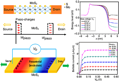
Because of the coupling between semiconducting and piezoelectric properties in wurtzite materials, strain-induced piezo-charges can tune the charge transport across the interface or junction, which is referred to as the piezotronic effect. For devices whose dimension is much smaller than the mean free path of carriers (such as a single atomic layer of MoS2), ballistic transport occurs. In this study, transport in the monolayer MoS2 piezotronic transistor is studied by presenting analytical solutions for two-dimensional (2D) MoS2. Furthermore, a numerical simulation for guiding future 2D piezotronic nanodevice design is presented.