Enhanced performance of PbPc photosensitive organic field effect transistors by inserting different-thickness pentacene inducing layers |
| |
| Affiliation: | 1. Institute of Microelectronics, School of Physical Science and Technology, Lanzhou University, Lanzhou 730000, China;2. College of Optical and Electronic Technology, China Jiliang University, Hangzhou 310018, China;1. Université de Pau et des Pays de l’Adour, IPREM (ECP, CNRS-UMR 5254), 2 Avenue Président Angot, 64053 Pau Cedex 09, France;2. Université de Pau et des Pays de l’Adour, IPREM (EPCP, CNRS-UMR 5254), 2 Avenue Président Angot, 64053 Pau Cedex 09, France;3. Université de Pau et des Pays de l’Adour, IPRA (CNRS-UMR 5142), Avenue de l’Université, BP 1155, 64013 Pau Cedex, France;4. CNRS, Institut de Chimie de Clermont – Ferrand (EP, ICCF, CNRS-UMR 6296), BP 80026, 63171 Aubière, France;5. CNRS, IPREM (EPCP, CNRS-UMR 5254), Hélioparc, 2 Avenue Président Angot, 64053 Pau Cedex 09, France;1. School of Physics and Microelectronic and Key Laboratory for Micro-Nano Physics and Technology of Hunan Province, Hunan University, Changsha 410082, China;2. Department of Electrical and Information Engineering, Hunan Institute of Engineering, Xiangtan 411101, China;1. School of Automation, Wuhan University of Technology, Wuhan 430070, China;2. Optimization and Systems Theory, KTH Royal Institute of Technology, Stockholm 10044, Sweden |
| |
| Abstract: | 
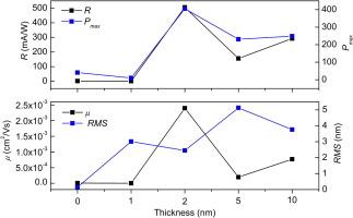
Lead phthalocyanine (PbPc) based photosensitive organic field effect transistors (PhOFETs) with different-thickness pentacene inducing layers (INLs) inserted between SiO2 and PbPc layer were fabricated and characterized. The photoelectric measurements demonstrate that the device with 2-nm-thick pentacene INL exhibits the largest photoresponsivity of 505.75 mA/W and maximum photo/dark current ratio of 405.35 in all devices. For this, we give an overall explanation that different-thickness INLs display different continuity and crystallinity and thus produce strong or weak template inducing. Especially, when the INL thickness (δ) is 2 nm a quasi-continuous and highly crystalline approximate-monolayer INL forms on SiO2 surface, which may play a strong role of template inducing, thus causing its upper PbPc film to demonstrate the strongest triclinic (3 0 0) line and the strongest NIR absorption in series PbPc films. When δ = 1 nm, pentacene does not form a continuous film. And when δ = 5 or 10 nm, a continuous multilayer INL with a declined crystallinity due to possible lattice mismatch forms on SiO2 surface and gives a weakened template inducing. Thereby, it can be recognized that inserting a pentacene INL can markedly enhance the performance of single layer PbPc PhOFET and the optimum INL thickness is proved ∼2 nm in present conditions. |
| |
| Keywords: | Photosensitive organic field effect transistors Pentacene Inducing layer Photoresponsivity |
| 本文献已被 ScienceDirect 等数据库收录! |
|

